| CPC G06F 1/266 (2013.01) [G05D 1/0246 (2013.01)] | 20 Claims |
|
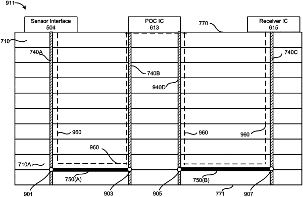
1. A method for routing a conductive path within a printed circuit board (PCB), comprising:
routing a first segment of a conductive path from a first location at a first signal layer to a second location at the first signal layer of a printed circuit board (PCB) utilizing a first segment of a transmission line, the PCB having a first surface and a second surface that is opposite the first surface;
routing a second segment of the conductive path from the second location at the first signal layer to a power-over-cable circuit disposed on the first surface of the PCB utilizing a first signal via, the first signal via extending from the first layer to the first surface of a substrate;
routing a third segment of the conductive path from the power-over-cable circuit to a third location at the first signal layer utilizing a second signal via, the second signal via extending from the first layer to the first surface of the substrate; and
routing a fourth segment of the conductive path from the third location at the first signal layer to a fourth location at the first signal layer utilizing a second segment of the transmission line, wherein the conductive path is coupled to an image sensor used to perceive an environment of an autonomous driving vehicle (ADV).
|