US 12,072,736 B2
Electronic device
Masaaki Hiroki, Kanagawa (JP); and Daisuke Furumatsu, Kanagawa (JP)
Assigned to Semiconductor Energy Laboratory Co., Ltd., Atsugi (JP)
Filed by SEMICONDUCTOR ENERGY LABORATORY CO., LTD., Atsugi (JP)
Filed on Sep. 15, 2023, as Appl. No. 18/368,624.
Application 18/368,624 is a continuation of application No. 18/081,000, filed on Dec. 14, 2022, granted, now 11,762,423.
Application 18/081,000 is a continuation of application No. 17/367,229, filed on Jul. 2, 2021, granted, now 11,531,372, issued on Dec. 20, 2022.
Application 17/367,229 is a continuation of application No. 17/083,432, filed on Oct. 29, 2020, granted, now 11,054,858, issued on Jul. 6, 2021.
Application 17/083,432 is a continuation of application No. 16/407,448, filed on May 9, 2019, granted, now 10,824,193, issued on Nov. 3, 2020.
Application 16/407,448 is a continuation of application No. 15/453,946, filed on Mar. 9, 2017, granted, now 10,289,158, issued on May 14, 2019.
Application 15/453,946 is a continuation of application No. 14/641,637, filed on Mar. 9, 2015, granted, now 9,594,402, issued on Mar. 14, 2017.
Claims priority of application No. 2014-050855 (JP), filed on Mar. 13, 2014.
Prior Publication US 2024/0004428 A1, Jan. 4, 2024
Int. Cl. G06F 1/16 (2006.01); H05K 5/00 (2006.01); H05K 7/00 (2006.01)
CPC G06F 1/163 (2013.01) [G06F 1/1635 (2013.01); G06F 1/1643 (2013.01); G06F 1/1652 (2013.01)] 4 Claims
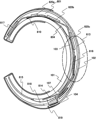
OG exemplary drawing
 
1. A display device comprising:
a display panel comprising a display surface to display an image and a back surface opposite to the display surface;
a flexible substrate electrically connected to the display panel;
a protective layer on the back surface side of the display panel; and
a housing,
wherein the display panel comprises a display region comprising a display element and a touch input sensor,
wherein the display region comprises a first region, a second region, and a third region between the first region and the second region,
wherein the third region is configured to be bent so that the first region and the second region overlap each other,
wherein the protective layer and the display panel overlap each other,
wherein the protective layer and the flexible substrate overlap each other,
wherein the flexible substrate is folded from the display surface side of the display panel to the back surface side of the display panel,
wherein a resin is between the protective layer and the flexible substrate,
wherein the resin and the third region overlap each other, and
wherein the resin is between the housing and the display panel.