US 12,072,732 B2
Circuit and method to set delay between two periodic signals with unknown phase relationship
Robert Wang, Richmond Hill (CA); Zhuobin Li, Markham (CA); Navid Yaghini, Pickering (CA); Hemesh Yasotharan, Toronto (CA); and Clifford Ting, Toronto (CA)
Assigned to Cadence Design Systems, Inc., San Jose, CA (US)
Filed by Cadence Design Systems, Inc., San Jose, CA (US)
Filed on May 19, 2023, as Appl. No. 18/320,384.
Application 18/320,384 is a continuation of application No. 17/587,882, filed on Jan. 28, 2022, granted, now 11,693,447.
Application 17/587,882 is a continuation of application No. 17/273,874, granted, now 11,269,372, issued on Mar. 8, 2022, previously published as PCT/CA2019/051249, filed on Sep. 6, 2019.
Claims priority of provisional application 62/728,376, filed on Sep. 7, 2018.
Prior Publication US 2023/0376067 A1, Nov. 23, 2023
This patent is subject to a terminal disclaimer.
Int. Cl. G06F 1/12 (2006.01); G06F 1/08 (2006.01); G06F 1/10 (2006.01)
CPC G06F 1/12 (2013.01) [G06F 1/08 (2013.01); G06F 1/10 (2013.01)] 20 Claims
OG exemplary drawing
 
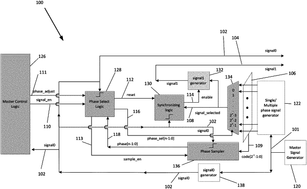
1. A circuit for providing a target phase delay between a first signal and a second signal, the first signal and second signal having a frequency relationship to a master signal, comprising:
a phase signal generator for receiving the master signal and generating one or more output signals based on the master signal; and
a phase select logic for:
receiving an enabling trigger signal having a phase relationship to the first signal; and
outputting one of the one or more phase signal generator output signals as a selected phase signal generator output signal based on the enabling trigger signal and the target phase delay; and
a second signal generator for generating the second signal based on a phase of the selected phase signal generator output signal.