| CPC G05F 3/262 (2013.01) [G05F 3/24 (2013.01); G05F 3/247 (2013.01)] | 20 Claims |

|
1. A voltage reference circuit, comprising:
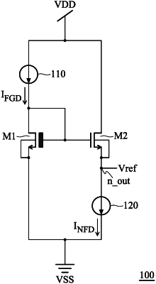
a first transistor formed by a plurality of second transistors;
a flipped-gate transistor, wherein a gate and a drain of the flipped-gate transistor are coupled to a gate and a drain of each of the second transistors;
a first current mirror unit configured to provide a first current to the flipped-gate transistor and a mirroring current in response to a bias current;
a second current mirror unit configured to drain a second current from the first transistor in response to the mirroring current; and
an output node coupled to a source of each of the second transistors and the second current mirror unit, and configured to output a reference voltage,
wherein size of the flipped-gate transistor is less than that of the first transistor.
|