| CPC G03F 7/705 (2013.01) [G05B 19/4097 (2013.01); H01L 21/0273 (2013.01); G05B 2219/45028 (2013.01)] | 19 Claims |

|
1. An exposure equipment comprising:
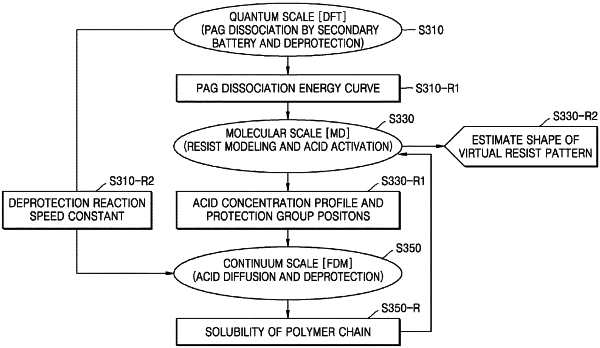
a simulation device configured to perform a multi-scale simulation for resist, the simulation device including:
a first simulation unit configured to perform a quantum scale simulation,
a second simulation unit configured to model a unit lattice cell of a virtual resist including polymer chains via a molecular scale simulation, and
a third simulation unit configured to perform a continuum scale simulation that identifies polymer chains that are soluble within the unit lattice cell; and
an exposure device configured to perform an exposure process using a resist selected based on a result from the simulation device,
wherein, by comparing a test resist pattern formed by the exposure device with a virtual resist pattern of the virtual resist estimated by the simulation device, when an error between the test resist pattern and the virtual resist pattern is in an allowable range, a resist pattern is formed on an object to be patterned by using the selected resist,
wherein the polymer chains identified as soluble by the continuum scale simulation of the third simulation unit are removed from the unit lattice cell being modeled by the molecular scale simulation of the second simulation unit.
|