| CPC G02F 1/23 (2013.01) [G01J 1/0488 (2013.01); G01J 1/4204 (2013.01); G02F 1/0121 (2013.01); H01L 31/02327 (2013.01); H01L 33/58 (2013.01); G02F 2203/055 (2013.01)] | 20 Claims |

|
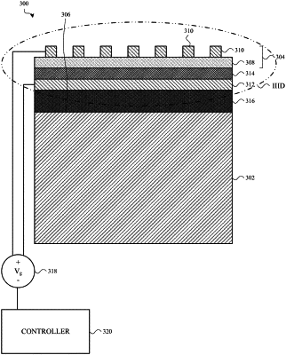
1. An optoelectronic device, comprising:
a pixel having a light-emitting surface and including,
a metasurface disposed over the light-emitting surface and including an array of conductive nanostructures disposed on a first conductive layer;
a second conductive layer disposed over the light-emitting surface; and
an insulating layer disposed over the light-emitting surface, between the metasurface and the second conductive layer;
a voltage source electrically connected to the metasurface and the second conductive layer; and
a controller configured to change a voltage between the metasurface and the second conductive layer.
|