US 12,072,599 B2
Pretreatment of transparent conductive oxide (TCO) thin films for improved electrical contact
Todd William Martin, Mountain View, CA (US); Abhishek Anant Dixit, Collierville, TN (US); Fabian Wilbur Strong, Hayward, CA (US); and Anshu Ajit Pradhan, Collierville, TN (US)
Assigned to View, Inc., San Jose, CA (US)
Filed by View, Inc., Milpitas, CA (US)
Filed on Aug. 18, 2023, as Appl. No. 18/452,427.
Application 16/826,086 is a division of application No. 14/893,504, granted, now 10,656,492, issued on May 19, 2020, previously published as PCT/US2014/042178, filed on Jun. 12, 2014.
Application 18/452,427 is a continuation of application No. 18/049,626, filed on Oct. 25, 2022, granted, now 11,762,254.
Application 18/049,626 is a continuation of application No. 16/826,086, filed on Mar. 20, 2020, granted, now 11,513,411, issued on Nov. 29, 2022.
Claims priority of provisional application 61/834,372, filed on Jun. 12, 2013.
Prior Publication US 2023/0393442 A1, Dec. 7, 2023
Int. Cl. G02F 1/153 (2006.01); G02F 1/155 (2006.01)
CPC G02F 1/1533 (2013.01) [G02F 1/155 (2013.01); G02F 2001/1536 (2013.01); G02F 2001/1555 (2013.01); G02F 2201/08 (2013.01)] 9 Claims
OG exemplary drawing
 
1. An optical device comprising:
a substantially transparent substrate;
a first transparent conductive oxide (TCO) layer disposed on the substantially transparent substrate;
a bus bar disposed on the first TCO layer in a bus bar pad expose area of the substantially transparent substrate;
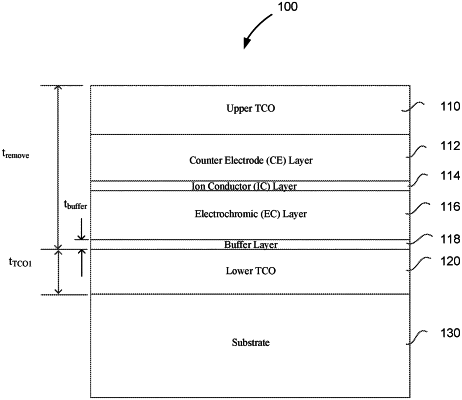
wherein a remaining area of the substantially transparent substrate includes a stack of one or more material layers comprising a titanium dioxide (TiO2) layer disposed on the first TCO layer; and
wherein the remaining area of the substantially transparent substrate also includes a second TCO layer disposed on top of the stack of one or more material layers.