| CPC G02F 1/153 (2013.01) [G02F 2201/501 (2013.01); G02F 2201/508 (2013.01)] | 15 Claims |

|
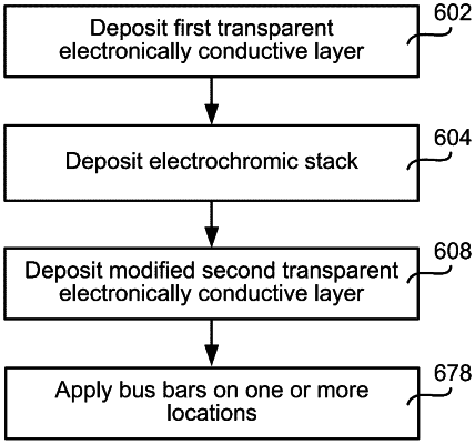
1. A method of fabricating an electrochromic device comprising an electrochromic stack between a first and a second transparent, electronically conductive layer configured to establish an electrical potential across the electrochromic stack and thereby cause optical switching of the electrochromic device, the method comprising:
(a) receiving a substrate with the first transparent, electronically conductive layer disposed on a surface of the substrate;
(b) fabricating the electrochromic stack on the first transparent, electronically conductive layer, wherein the electrochromic stack comprises an electrochromic layer and a counter electrode layer;
(c) forming the second transparent, electronically conductive layer on the electrochromic stack;
(d) forming a bus bar on a region of the second transparent, electronically conductive layer, wherein the region is over the first transparent, electronically conductive layer; and
(e) performing a short mitigation operation that
(i) prevents electrical shorts from forming between the second transparent, electronically conductive layer and a layer of the electrochromic device in the region underneath the bus bar, and/or
(ii) removes electrical shorts that have formed between the second transparent, electronically conductive layer and a layer of the electrochromic device in the region underneath the bus bar,
wherein (e) is performed without substantially deactivating the electrochromic device in the region under the bus bar after fabricating the electrochromic stack and the second transparent, electronically conductive layer.
|