| CPC G02F 1/1368 (2013.01) [G02F 1/136209 (2013.01); G02F 1/136277 (2013.01); G02F 1/136286 (2013.01); H01L 29/78633 (2013.01); H01L 29/78672 (2013.01); H10K 50/865 (2023.02); H10K 59/131 (2023.02)] | 20 Claims |

|
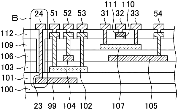
1. A display device comprising:
a substrate;
a first thin film transistor, including a polysilicon semiconductor layer, formed on the substrate;
a second thin film transistor, including an oxide semiconductor layer, formed on the substrate;
a first light shading film, located between the polysilicon semiconductor layer and the substrate, and opposing to the polysilicon semiconductor layer;
a second light shading film located between the oxide semiconductor layer and the substrate, and opposing to the oxide semiconductor layer;
a first insulating film, including at least one layer, formed on the first light shading film;
a second insulating film, including at least one layer, formed on the first insulating film;
a third insulating film, including at least one layer, formed on the second insulating film;
a first through hole, opposing to the first light shading film, penetrating the second insulating film, and not penetrating the first insulating film and the third insulating film;
a second through hole, opposing to the first light shading film, penetrating the first insulating film and the third insulating film, and including an upper opening and a lower opening, the upper opening being farther from the substrate compared to the lower opening and existing in the first through hole; and
a first conductive component, formed on the third insulating film, and electrically connecting with the first light shading film via the second through hole,
wherein
the first conductive component is in direct contact with the first insulating film and is not in direct contact with the second insulating film, and
at least a part of the first conductive component overlaps with the second insulating film.
|