| CPC G02F 1/136295 (2021.01) [G02F 1/13338 (2013.01); G02F 1/1343 (2013.01); G02F 1/136209 (2013.01); G02F 1/136227 (2013.01); G02F 1/1368 (2013.01)] | 20 Claims |

|
1. A display panel, wherein the display panel comprises a display region and a non-display region located on a periphery of the display region; wherein the display panel comprises:
an underlay;
an array driver layer located on the underlay and comprising a gate electrode layer and a source and drain electrode layer; and
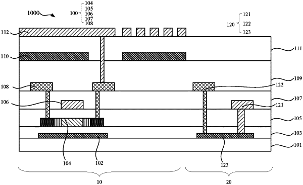
a signal line comprising an adaptor portion located in the non-display region, wherein the adaptor portion comprises a first wire section disposed in a same layer with the gate electrode layer, a second wire section disposed in a same layer with the source and drain electrode layer, and a bridge portion electrically connected to the first wire section and the second wire section;
wherein the first wire section, the second wire section, and the bridge portion are disposed in different layers;
wherein the adaptor portion further comprises a first via hole and a second via hole, the first wire section is electrically connected to the bridge portion through a connection metal in the first via hole, and the second wire section is electrically connected to the bridge portion through a connection metal in the second via hole;
wherein the array driver layer further comprises a semiconductor layer, the source and drain electrode layer of the array driver layer is electrically connected to the semiconductor layer through a connection metal in a third via hole, a contact impedance of the connection metal in the third via hole is greater than a contact impedance of the connection metal in the first via hole or the connection metal in the second via hole.
|