| CPC G02F 1/13394 (2013.01) [G02F 1/133377 (2013.01); G02F 1/136209 (2013.01); G02F 1/136286 (2013.01); G02F 1/1368 (2013.01)] | 19 Claims |
|
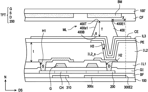
1. An electronic device, comprising:
a substrate;
a semiconductor layer, disposed on the substrate and has a channel area;
a light blocking layer, disposed between the substrate and the channel area; and
a spacer, disposed on the semiconductor layer,
wherein the light blocking layer overlaps with the spacer and the channel area,
wherein the substrate has a surface, a direction is parallel to the surface of the substrate, the spacer has a first thickness (T), the spacer comprises a first side wall and an upper bottom surface, the first side wall and the direction have a first included angle (θ), the upper bottom surface has a first edge, the light blocking layer has a second edge near the first edge, and the first edge and the second edge have a first distance (X) along the direction,
wherein the first thickness (T), the first included angle (θ), and the first distance (X) satisfy a relational expression below:
T*cot(θ)≤X≤T*cot(θ)+15 μm.
|