| CPC G02F 1/133512 (2013.01) [G02F 1/133614 (2021.01)] | 20 Claims |

|
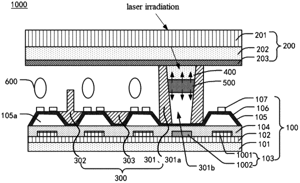
1. A display panel, comprising a first substrate and a second substrate disposed opposite to the first substrate;
wherein the first substrate comprises:
a first base substrate;
a thin film transistor layer disposed on the first base substrate and comprising a photosensitive transistor;
a color resist layer disposed on the first base substrate and comprising a plurality of color resist blocks arranged in an array, wherein the photosensitive transistor is disposed in a gap between at least two adjacent ones of the color resist blocks; and
a pair of first light-shielding support columns disposed between the first substrate and the second substrate, wherein a first end of the pair of the first light-shielding support columns is connected to the first substrate, a second end of the pair of the first light-shielding support columns is connected to the second substrate, and the pair of the first light-shielding support columns is disposed opposite to the photosensitive transistor; and
wherein a laser penetrating layer and a photoluminescent layer that correspond to the pair of the first light-shielding support columns are disposed on the second substrate, and the photoluminescent layer is disposed on a side of the laser penetrating layer away from the second substrate.
|