| CPC G02B 6/136 (2013.01) [C03C 17/02 (2013.01); G02B 6/1223 (2013.01); G02B 2006/12038 (2013.01)] | 20 Claims |
|
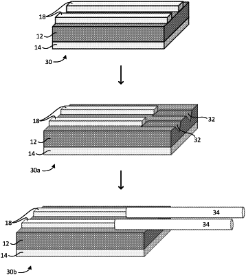
1. A process for forming glass planar waveguide structure, the process comprising:
producing or otherwise obtaining a fusion drawn glass laminate comprising a core glass layer and a first clad glass layer and a second clad glass layer;
removing or thinning portions of the second clad glass layer leaving remaining or thicker portions of the second clad glass layer arranged in a first planar waveguide pattern; and
etching V-grooves in alignment with one or more of the remaining or thicker portions of the second clad glass layer.
|