| CPC G01S 17/08 (2013.01) [G01B 11/22 (2013.01); G01S 7/4816 (2013.01); G01S 17/89 (2013.01); H01L 27/14623 (2013.01); H01L 27/14627 (2013.01); H01L 27/14629 (2013.01); H01L 27/1463 (2013.01); H01L 27/14636 (2013.01); H01L 27/14649 (2013.01)] | 20 Claims |

|
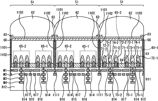
1. A light-receiving element, comprising:
an on-chip lens;
a wiring layer; and
a semiconductor layer arranged between the on-chip lens and the wiring layer,
wherein the semiconductor layer includes:
a first pixel;
a second pixel adjacent to the first pixel; and
a first pixel separation portion that separates the semiconductor layer at least up to a predetermined depth between the first pixel and the second pixel,
wherein the first pixel separation portion includes:
an inter-pixel light-shielding film:
a non-tapered through electrode connected to the inter-pixel light-shielding film; and
a transparent conductive film provided between the inter-pixel light-shielding film and a top portion of the non-tapered through electrode,
wherein the first pixel includes;
a first voltage application portion connected to first control wiring;
a second voltage application portion connected to second control wiring;
a first charge detection portion arranged around the first voltage application portion; and
a second charge detection portion arranged around the second voltage application portion,
wherein the second pixel includes:
a third voltage application portion connected to third control wiring;
a fourth voltage application portion connected to fourth control wiring;
a third charge detection portion arranged around the third voltage application portion; and
a fourth charge detection portion arranged around the fourth voltage application portion, and
wherein the first pixel separation portion includes a fifth voltage application portion connected to fifth control wiring.
|