| CPC G01R 31/2656 (2013.01) [G01R 31/2891 (2013.01); G01R 31/2894 (2013.01); G01R 31/311 (2013.01); H01L 22/00 (2013.01)] | 11 Claims |

|
1. A semiconductor failure analysis device comprising:
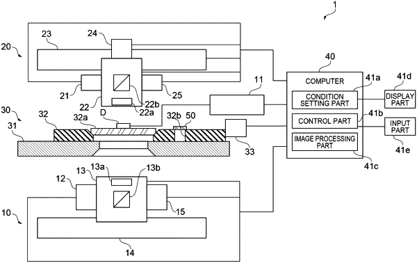
an analyzer in which a first optical detector receives first light from a semiconductor device via a first optical system, and the first optical system is moved relative to the semiconductor device by a first driver;
a marking part in which a second optical detector receives second light from the semiconductor device via a second optical system, the semiconductor device is irradiated with laser light via the second optical system, and the second optical system is moved relative to the semiconductor device by a second driver;
a device arrangement part having a chuck disposed between the analysis part and the marking part to hold the semiconductor device and provided with a target that aligns an optical axis of the first optical system with an optical axis of the second optical system, the chuck being moved relative to the analysis part and the marking part by a third driver; and
a controller configured to output a command to the analyzer, the marking part, and the device arrangement part,
wherein the target is detectable by the first optical detector from one side of the target and is detectable by the second optical detector from the other side of the target, and
the controller outputs an alignment command that moves the chuck to a position at which the target is detectable by the first optical detector and then aligns the optical axis of the second optical system with the optical axis of the first optical system with the target as a reference to the marking part and the device arrangement part, and outputs a marking command that irradiates a marking position set on the semiconductor device with the laser light in a state in which a positional relationship between the optical axis of the first optical system and the optical axis of the second optical system is maintained to the marking part and the device arrangement part.
|