| CPC G01R 29/26 (2013.01) [G01R 31/31709 (2013.01); H03K 19/01855 (2013.01); H03L 7/07 (2013.01); H03L 7/08 (2013.01); G01R 29/0276 (2013.01)] | 20 Claims |

|
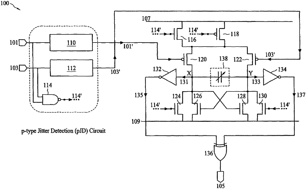
1. A noise detection circuit, comprising:
a first component configured to receive a clock signal;
a second component configured to receive a reference clock signal; and
a latch circuit, coupled to the first component at a first node and coupled to the second component at a second node, and configured to latch logic states of voltage levels at the first and second nodes, respectively, based on a timing difference between transition edges of the clock signal and the reference clock signal,
wherein when the timing difference between transition edges of the clock signal and the reference clock signal exceeds a pre-defined timing offset threshold, the latch circuit is configured to latch the logic states of the voltage levels at the first and second nodes.
|