| CPC C25D 21/12 (2013.01) [C25D 5/54 (2013.01); C25D 7/12 (2013.01); C25D 17/001 (2013.01); C25D 17/02 (2013.01)] | 20 Claims |
|
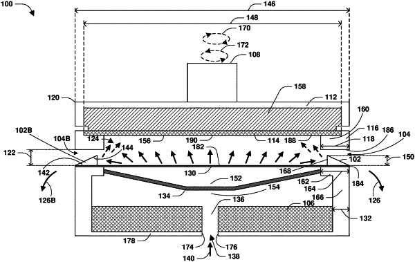
1. A method of plating a wafer, comprising:
introducing, via an inlet of an electroplating chamber, a plating solution into a plating region within which the wafer is plated, wherein:
the plating region is defined by the electroplating chamber; and
the plating solution is used for plating the wafer;
inhibiting removal of the plating solution from the plating region by reflecting some of the plating solution using a barrier;
sensing a parameter of a plating process performed for plating the wafer with anode material of an anode within the electroplating chamber, wherein the parameter comprises at least one of a plating thickness, a pressure of the plating solution, or a direction of flow of the plating solution; and
adjusting a position of the barrier based upon the parameter, wherein the position of the barrier corresponds to at least one of a vertical position of the barrier or a horizontal position of the barrier.
|