| CPC B81B 7/0051 (2013.01) [B81C 1/00269 (2013.01); H03H 3/007 (2013.01); H03H 9/171 (2013.01); B81B 2201/0271 (2013.01); B81B 2207/053 (2013.01); B81C 2203/0118 (2013.01); B81C 2203/037 (2013.01)] | 20 Claims |
|
16. A device, comprising:
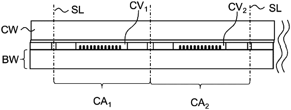
a base wafer comprising a top surface, wherein the top surface comprises an array of device areas assigned to respective micro-acoustic devices, and wherein the respective micro-acoustic devices form a frame structure on the top surface that encloses corresponding device areas of the array of device areas with respective electric structures; and
a cap wafer having a coefficient of thermal expansion (CTE) adapted to a CTE of the base wafer, wherein the cap wafer has an underside coated with a UV-curable polymer coating, and wherein the cap wafer is wafer-bonded to the frame structure via the UV-curable polymer coating.
|