| CPC A61N 1/0543 (2013.01) [A61N 1/36046 (2013.01); H10K 30/20 (2023.02); A61N 1/0551 (2013.01); A61N 1/36062 (2017.08); H10K 85/311 (2023.02); H10K 85/621 (2023.02)] | 18 Claims |

|
1. A method for stimulating an excitable tissue or cell, the method comprising:
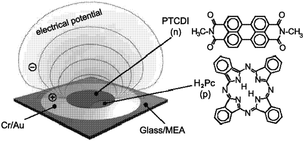
placing or positioning into, onto or in the contact with a target excitable tissue or cell at least one photoresponse device comprising a multilayer comprising at least one metal or a conductive material layer and p-n/n-p structure layered thereon, the p-n/n-p structure comprising semiconducting organic nanocrystals, and focusing light with a wavelength between 400-2,000 nanometers onto the device, to thereby cause a photoresponse effect comprising an electrical pulse, and stimulation of the excitable tissue or cells, when said device and said tissue or cells are in a physiological medium;
wherein the p-n/n-p structure in said device is in continuous contact with the at least one metal or the conductive material layer,
wherein the at least one metal or the conductive material layer is configured to be in electrical contact with the physiological medium in which the device operates, the p-n/n-p structure comprising a combination of two or more organic semiconductor pigments, at least one being selected amongst electron donor materials comprising a p-type material, and at least one other selected amongst electron accepting materials comprising an n-type material; and
wherein the device is a photocapacitor.
|