| CPC H10K 71/00 (2023.02) [H10K 50/844 (2023.02); H10K 59/12 (2023.02); H10K 59/1201 (2023.02); H10K 71/861 (2023.02)] | 25 Claims |
|
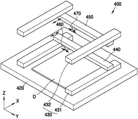
1. An apparatus for manufacturing a display device, the apparatus comprising:
a mounting unit configured to receive a display substrate;
an inspection unit movably arranged on the mounting unit and configured to inspect a portion of an organic encapsulation layer of the display substrate to determine whether it is a defective portion, wherein the inspection unit is configured to detect a three-dimensional shape including voids and protrusions of the defective portion; and
a repair unit movably arranged on the mounting unit and configured to repair the detective portion based on the detected three-dimensional shape, including to remove material from a detected protrusion of the defective portion and to supply an organic material to a defective void of the defective portion.
|