| CPC H10K 59/131 (2023.02) [H10K 59/122 (2023.02); H10K 59/1216 (2023.02)] | 26 Claims |
|
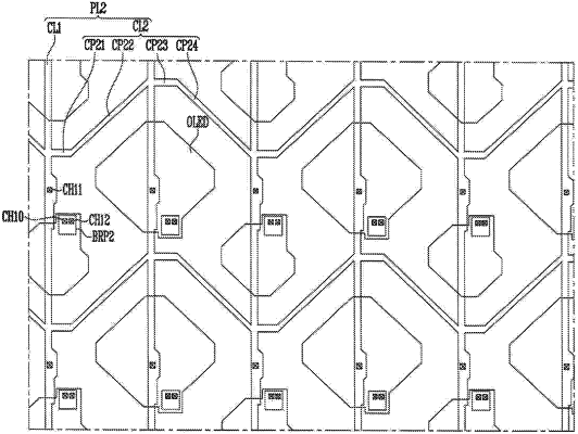
1. A display device comprising:
a substrate including a pixel region;
a pixel disposed in the pixel region and arranged in pixel rows, the pixel rows including a first pixel row including first pixels, a second pixel row including second pixels, and a third pixel row including third pixels, wherein the third row is disposed between the first row and the second row;
a data line and a scan line connected to the pixel, the scan line substantially extending in a first direction and the data line substantially extending in a second direction different from the first direction; and
a first metal layer including first metal portions and second metal portions, wherein:
the first metal portions substantially extend in the second direction,
the second metal portions substantially extend in the first direction and are electrically connected to the first metal portions,
the pixel includes at least one transistor and a light emitting element including an anode electrically connected to the at least one transistor,
a first insulating layer is between the first metal portions and the data line,
the first pixels include a first pixel disposed in a first pixel column,
the second pixels include a second pixel disposed in the first pixel column,
the third pixels include a third pixel disposed in a second column adjacent to the first pixel column,
each of the first metal portions:
includes a first-first metal portion that overlaps with the first pixel and the second pixel, and
includes a second-first metal portion that overlaps with the third pixel, and
the first pixel column and the second pixel column are alternately arranged in the first direction.
|