| CPC H10K 59/126 (2023.02) [H01L 29/78633 (2013.01); H10K 50/865 (2023.02); H10K 59/00 (2023.02); H10K 59/1213 (2023.02); H10K 59/131 (2023.02); H10K 59/352 (2023.02)] | 10 Claims |
|
1. A display device, comprising:
a plurality of pixels;
a conductive pattern;
a first scan line and a second scan line; and
a driving voltage line crossing the first scan line and the second scan line,
wherein each of the plurality of pixels comprising a pixel electrode and a plurality of transistors,
wherein the plurality of transistors comprises:
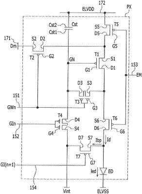
a first transistor including a first gate electrode, a first channel region overlapping the first gate electrode in a plan view, and a first source region and a first drain region opposing each other with respect to the first channel region;
a second transistor including a second gate electrode of the first scan line, a second channel region overlapping the second gate electrode, a second drain region electrically connected to the first gate electrode, and a second source region opposing the second drain region with respect to the second channel region;
a third transistor including a third gate electrode of the first scan line, a third channel region overlapping the third gate electrode, a third drain region extending from the second source region, and a third source region opposing the third drain region with respect to the third channel region; and
a fourth transistor including a fourth gate electrode of the second scan line, a fourth channel region overlapping the fourth gate electrode, a fourth drain region electrically connected to the first gate electrode and extending from the second drain region, and a fourth source region opposing the fourth drain region with respect to the fourth channel region,
wherein the driving voltage line overlaps the fourth channel region,
wherein the pixel electrode or the conductive pattern overlaps at least a portion of the second source region or the third drain region,
wherein the plurality of pixels comprises first color pixels, second color pixels, and third color pixels,
wherein the pixel electrodes of the first color pixels and the pixel electrodes of the second color pixels are alternately arranged in a horizontal direction,
wherein the pixel electrodes of the first color pixels and the pixel electrodes of the third color pixels are alternately arranged in a first diagonal direction with respect to the horizontal direction,
wherein the pixel electrodes of the second color pixels and the pixel electrodes of the third color pixels are alternately arranged in a second diagonal direction with respect to the horizontal direction,
wherein areas of the pixel electrodes of the first color pixels, the second color pixels and the third color pixels are different from one another, and
wherein the third source region of the third transistor is directly connected to the first drain region of the first transistor.
|