US 11,744,120 B2
Display device and manufacturing method thereof
Hyun Min Cho, Hwaseong-si (KR); Tae Sung Kim, Incheon (KR); Yun Jong Yeo, Hwaseong-si (KR); Ji Youn Nam, Seoul (KR); and Hee Min Yoo, Hwaseong-si (KR)
Assigned to SAMSUNG DISPLAY CO., LTD., Gyeonggi-Do (KR)
Filed by Samsung Display Co., LTD., Yongin-si (KR)
Filed on Mar. 25, 2021, as Appl. No. 17/212,046.
Claims priority of application No. 10-2020-0066613 (KR), filed on Jun. 2, 2020.
Prior Publication US 2021/0376023 A1, Dec. 2, 2021
Int. Cl. H01L 27/32 (2006.01); H01L 51/56 (2006.01); H10K 59/124 (2023.01); H10K 59/122 (2023.01); H10K 59/123 (2023.01); H10K 71/00 (2023.01); H10K 59/12 (2023.01)
CPC H10K 59/124 (2023.02) [H10K 59/122 (2023.02); H10K 59/123 (2023.02); H10K 71/00 (2023.02); H10K 59/1201 (2023.02)] 17 Claims
OG exemplary drawing
 
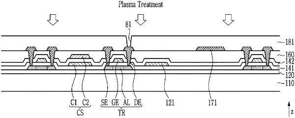
1. A manufacturing method of a display device, comprising:
forming a transistor on a substrate;
forming an organic insulating layer on the transistor; and
performing a plasma treatment on the organic insulating layer,
wherein the organic insulating layer includes an acryl-based polymer, and the plasma treatment is performed by using helium gas or argon gas,
wherein a methane content increases in the organic insulating layer by the plasmas treatment.