| CPC H10K 59/123 (2023.02) [H10K 59/131 (2023.02); H01L 27/1244 (2013.01); H10K 59/1213 (2023.02)] | 20 Claims |
|
1. A display device, comprising:
a pixel circuit;
a first line disposed on the pixel circuit, the first line extending in a first direction;
a second line disposed on a same layer as the first line and extending in the first direction, the second line is spaced apart from the first line in a second direction that crosses the first direction;
a light emitting element disposed on the first line and the second line; and
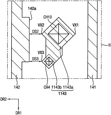
a connection pattern disposed on a same layer as the first line and the second line and disposed between the first line and the second line in the second direction, the connection pattern directly contacts the light emitting element and is configured to connect the pixel circuit and the light emitting element, the connection pattern having a polygonal shape including at least six sides,
wherein a single first vertex of the connection pattern is positioned at a shortest distance from the first line to the connection pattern and all other portions of the connection pattern except for the first vertex are positioned farther from the first line than the first vertex.
|