| CPC H10K 59/122 (2023.02) [H10K 50/844 (2023.02); H10K 50/854 (2023.02); H10K 59/38 (2023.02); H10K 71/00 (2023.02)] | 18 Claims |
|
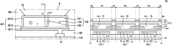
1. A display device comprising:
a first base substrate including a light-emitting area and a non-light-emitting area around the light-emitting area;
a wavelength conversion pattern disposed on the first base substrate, in the light-emitting area; and
a light-emitting element layer disposed on the wavelength conversion pattern, the light-emitting element layer including:
a pixel electrode including:
a first conductive pattern disposed between the wavelength conversion pattern and the first base substrate; and
a second conductive pattern disposed on the wavelength conversion pattern and spaced apart from the first conductive pattern;
an organic light-emitting layer disposed on the second conductive pattern; and
a common electrode disposed on the organic light-emitting layer.
|