| CPC H10K 50/844 (2023.02) [H10K 50/8426 (2023.02); H10K 59/12 (2023.02); H10K 59/131 (2023.02); H10K 59/88 (2023.02); H10K 77/111 (2023.02); H10K 2102/311 (2023.02)] | 9 Claims |
|
1. A display device comprising:
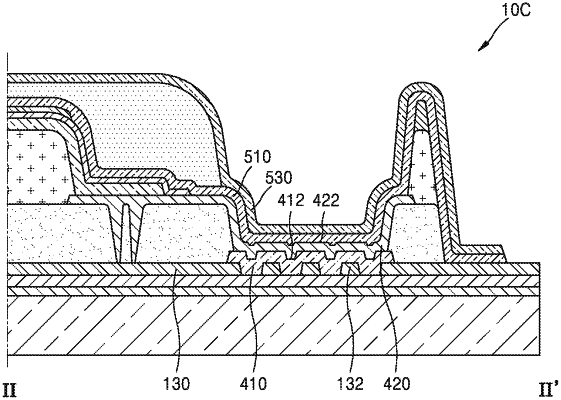
a substrate comprising a display area and a peripheral area outside the display area;
a first insulating layer on the substrate across the display area and the peripheral area;
a pixel electrode on the first insulating layer in the display area;
an opposite electrode on the pixel electrode;
an electrode power supply line in the peripheral area, and electrically connected to the opposite electrode; and
a thin film transistor electrically connected to the pixel electrode,
wherein, in a region where the substrate overlaps the electrode power supply line, at least one layer under the electrode power supply line comprises a repeating pattern,
wherein the electrode power supply line comprises an uneven structure comprising multiple high points and multiple low points corresponding to the repeating pattern, and
wherein an interlayer insulating layer on a gate electrode of the thin film transistor extends toward the peripheral area, and comprises the repeating pattern in the peripheral area.
|