| CPC H10K 50/17 (2023.02) [H10K 50/11 (2023.02); H10K 50/15 (2023.02); H10K 59/122 (2023.02); H10K 2101/40 (2023.02)] | 15 Claims |
|
1. A display device, comprising:
a substrate;
a first electrode on the substrate;
a pixel defining layer exposing an upper surface of the first electrode and covering a side of the first electrode;
a second electrode on the first electrode;
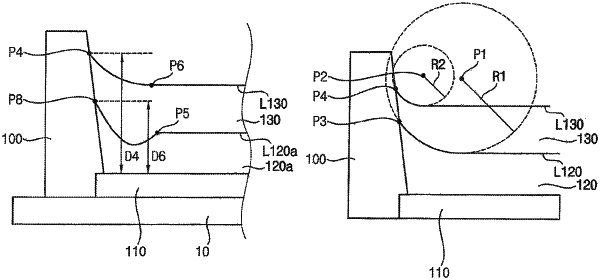
a hole injection layer between the first electrode and the second electrode, the hole injection layer having an upper surface having a side protruding in a direction toward the second electrode;
a light emitting layer between the hole injection layer and the second electrode, the light emitting layer having an upper surface having a side protruding in the direction toward the second electrode; and
an electron injection layer between the light emitting layer and the second electrode,
wherein a shortest distance in a vertical direction between a first fixing point defined at a boundary between the side of the upper surface of the hole injection layer and the pixel defining layer and a second fixing point defined at a boundary between the side of the upper surface of the light emitting layer and the pixel defining layer is greater than or equal to an insulation breakdown limit distance of the light emitting layer, and
wherein a radius of curvature of a curvature portion of the side of the upper surface of the hole injection layer is greater than a radius of curvature of a curvature portion of the side of the upper surface of the light emitting layer.
|