| CPC H10B 63/845 (2023.02) [G11C 13/0004 (2013.01); G11C 13/004 (2013.01); H10B 63/34 (2023.02); H10N 70/231 (2023.02); H10N 70/8828 (2023.02); G11C 2213/71 (2013.01); G11C 2213/79 (2013.01)] | 20 Claims |
|
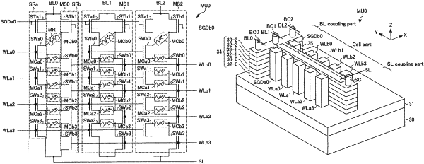
1. A memory device comprising:
a first variable resistance layer extending in a first direction;
a first semiconductor layer extending in the first direction and being in contact with a first main surface of the first variable resistance layer, the first main surface facing a second direction intersecting the first direction;
a second semiconductor layer extending in the first direction and being in contact with a second main surface of the first variable resistance layer, the second main surface facing the second direction;
a first word line extending in a third direction intersecting the first and second directions;
a second word line extending in the third direction and being adjacent to the first word line along the first direction;
a third word line extending in the third direction, being adjacent to the first and second word lines with the first semiconductor layer, the first variable resistance layer, and the second semiconductor layer interposed therebetween, and provided between the first word line and the second word line in the first direction;
a first insulating layer provided between the first semiconductor layer and the first word line;
a second insulating layer provided between the first semiconductor layer and the second word line; and
a third, insulating layer provided between the second semiconductor layer and the third word line,
wherein
in the first variable resistance layer, a first region including a shortest path connecting the first word line and the third word line functions as a first memory cell, and a second region including a shortest path connecting the third word line and the second word line functions as a second memory cell.
|