| CPC H10B 51/20 (2023.02) [H01L 29/516 (2013.01); H10B 43/20 (2023.02); H10B 43/30 (2023.02); H10B 43/40 (2023.02); H10B 51/30 (2023.02); H10B 51/40 (2023.02)] | 20 Claims |
|
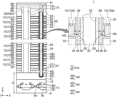
1. A semiconductor device comprising:
a stacked structure including interlayer insulating layers and gate electrodes alternately stacked in a vertical direction;
a core region extending in the vertical direction in the stacked structure;
a channel layer on a side surface of the core region and facing the gate electrodes and the interlayer insulating layers;
a second dielectric layer, a data storage layer and a first dielectric layer sequentially stacked on the side surface of the channel layer, the second dielectric layer, the data storage layer and the first dielectric layer being between the channel layer and the gate electrodes, and the second dielectric layer being in contact with the channel layer; and
an anti-ferroelectric layer including a portion interposed between the first dielectric layer and a first gate electrode of the gate electrodes,
wherein the anti-ferroelectric layer has a dynamic dielectric constant and comprises an anti-ferroelectric material having a tetragonal phase, and
each of the first and second dielectric layers includes an oxide layer having a dielectric constant lower than a lowest dielectric constant of the anti-ferroelectric layer.
|