US 11,744,081 B1
Ferroelectric device film stacks with texturing layer which is part of a bottom electrode, and method of forming such
Niloy Mukherjee, San Ramon, CA (US); Ramamoorthy Ramesh, Moraga, CA (US); Sasikanth Manipatruni, Portland, OR (US); James Clarkson, Berkeley, CA (US); FNU Atiquzzaman, Orinda, CA (US); Gabriel Antonio Paulius Velarde, San Leandro, CA (US); and Jason Y. Wu, Albany, CA (US)
Assigned to Kepler Computing Inc., San Francisco, CA (US)
Filed by Kepler Computing Inc., San Francisco, CA (US)
Filed on May 7, 2021, as Appl. No. 17/315,139.
Application 17/315,139 is a continuation of application No. 17/315,111, filed on May 7, 2021, granted, now 11,659,714.
This patent is subject to a terminal disclaimer.
Int. Cl. H10B 51/20 (2023.01); H10B 51/10 (2023.01); H10B 51/40 (2023.01)
CPC H10B 51/20 (2023.02) [H10B 51/10 (2023.02); H10B 51/40 (2023.02)] 19 Claims
OG exemplary drawing
 
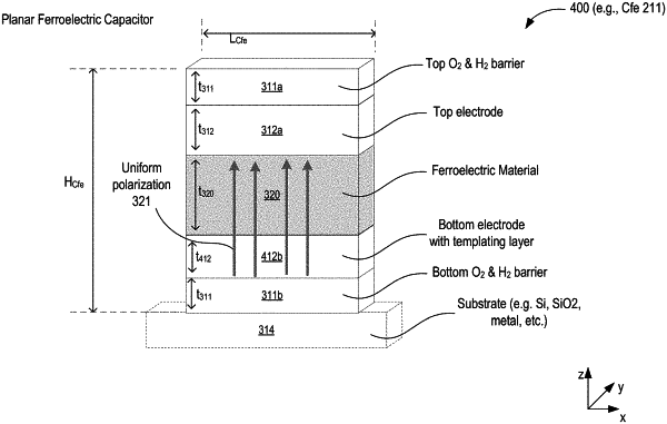
1. A ferroelectric device comprising:
a first structure comprising a ferroelectric material;
a second structure over the first structure, the second structure comprising metallic electrode; and
a third structure under the first structure, the third structure to induce crystallographic orientation in the first structure and to provide conductive characteristics of a metallic electrode, wherein the third structure comprises a super lattice of at least two materials including an intermetallic material and a metallic electrode material.