| CPC H10B 43/50 (2023.02) [H10B 43/10 (2023.02); H10B 43/27 (2023.02)] | 20 Claims |
|
1. A semiconductor device comprising:
a substrate having a first region and a second region;
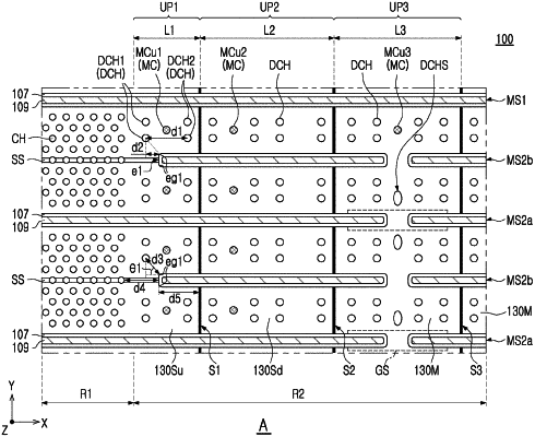
a plurality of gate electrodes stacked and spaced apart from each other in a first direction, perpendicular to an upper surface of the substrate in the first region and including a plurality of pad regions provided by some of the plurality of gate electrodes extending in different lengths along a second direction, perpendicular to the first direction in the second region;
a plurality of first separation regions penetrating the plurality of gate electrodes in the first and second regions, extending in the second direction, and spaced apart from each other in a third direction, perpendicular to the first and second directions;
a plurality of second separation regions penetrating the plurality of gate electrodes between the plurality of first separation regions and including second main separation regions extending in the second direction, from the first region, and second auxiliary separation regions extending in the second direction, from the second region;
a plurality of channel structures penetrating the plurality of gate electrodes, extending vertically on the substrate, and arranged in the first region; and
a plurality of dummy channel structures penetrating the plurality of gate electrodes, extending vertically on the substrate, and arranged in the second region,
wherein the plurality of pad regions include first pad regions provided by an uppermost first gate electrode among the plurality of gate electrodes and second pad regions provided by a second gate electrode below the uppermost first gate electrode,
the plurality of dummy channel structures include a pair of first dummy channel structures penetrating the first pad regions and arranged adjacent to the first region and a pair of second dummy channel structures arranged adjacent to a first end of the uppermost first gate electrode,
the second auxiliary separation regions are arranged between the first pad regions adjacent to each other and have a first edge portion adjacent to the first dummy channels structure and a first end point closest to the first region on the first edge portion,
a central axis of each of the first dummy channel structures is spaced apart from a central axis of each of the second dummy channel structures by a first distance in the second direction, and
the first edge portion of each of the second auxiliary separation regions is spaced apart from a central axis of each of the first dummy channel structures by a second distance, smaller than the first distance, in a fourth direction, diagonal to the second direction.
|