| CPC H10B 43/35 (2023.02) [H10B 43/27 (2023.02)] | 20 Claims |
|
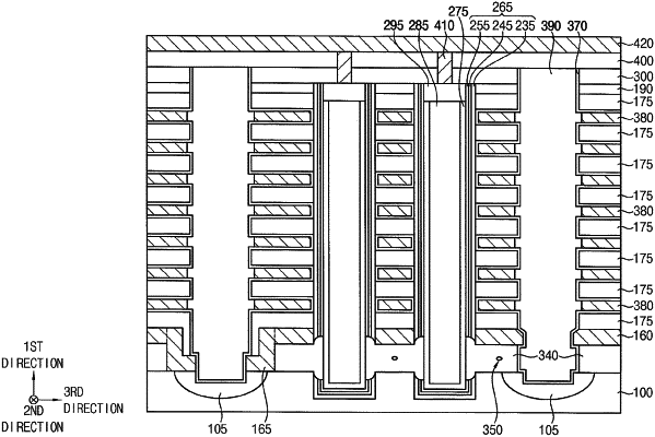
1. A vertical memory device, comprising:
a channel on a substrate, the channel extending in a vertical direction substantially perpendicular to an upper surface of the substrate;
a charge storage structure on an outer sidewall of the channel, the charge storage structure including a tunnel insulation pattern, a charge storage pattern and a first blocking pattern sequentially stacked in a horizontal direction substantially parallel to the upper surface of the substrate; and
gate electrodes spaced apart from each other in the vertical direction on the substrate, each of the gate electrodes surrounding the charge storage structure,
wherein the first blocking pattern includes silicon oxide containing a halogen element, and
wherein a concentration of the halogen element included in the first blocking pattern gradually decreases from an outer sidewall facing a corresponding one of the gate electrodes toward an inner sidewall facing the charge storage pattern.
|