US 11,744,075 B2
Semiconductor memory device and method for manufacturing the same
Yoshiaki Fukuzumi, Yokkaichi (JP); Shinya Arai, Yokkaichi (JP); Masaki Tsuji, Yokkaichi (JP); Hideaki Aochi, Yokkaichi (JP); and Hiroyasu Tanaka, Yokkaichi (JP)
Assigned to Kioxia Corporation, Minato-ku (JP)
Filed by Kioxia Corporation, Minato-ku (JP)
Filed on Feb. 16, 2022, as Appl. No. 17/672,819.
Application 17/672,819 is a continuation of application No. 17/335,214, filed on Jun. 1, 2021, granted, now 11,296,114.
Application 17/335,214 is a continuation of application No. 16/918,005, filed on Jul. 1, 2020, granted, now 11,063,064, issued on Jul. 13, 2021.
Application 16/918,005 is a continuation of application No. 16/596,892, filed on Oct. 9, 2019, granted, now 10,741,583, issued on Aug. 11, 2020.
Application 16/596,892 is a continuation of application No. 16/138,619, filed on Sep. 21, 2018, granted, now 10,497,717, issued on Dec. 3, 2019.
Application 16/138,619 is a continuation of application No. 15/345,790, filed on Nov. 8, 2016, granted, now 10,115,733, issued on Oct. 30, 2018.
Application 15/345,790 is a continuation of application No. 14/614,588, filed on Feb. 5, 2015, granted, now 9,520,407, issued on Dec. 13, 2016.
Claims priority of application No. 2014-021747 (JP), filed on Feb. 6, 2014.
Prior Publication US 2022/0173124 A1, Jun. 2, 2022
This patent is subject to a terminal disclaimer.
Int. Cl. H10B 43/27 (2023.01); H01L 29/66 (2006.01); H01L 29/792 (2006.01); H10B 43/10 (2023.01); H10B 43/50 (2023.01); H01L 29/423 (2006.01)
CPC H10B 43/27 (2023.02) [H01L 29/42344 (2013.01); H01L 29/66833 (2013.01); H01L 29/7926 (2013.01); H10B 43/10 (2023.02); H10B 43/50 (2023.02)] 20 Claims
OG exemplary drawing
 
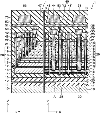
1. A non-volatile memory device comprising: a substrate; an insulation film provided above the substrate; a first conductive layer provided above the insulation film; an upper interconnect structure including a first interconnection; electrodes provided between the first conductive layer and the upper interconnect structure, the electrodes being arranged in a first direction perpendicular to the first conductive layer to constitute a stacked body and functioning control gates for memory cells; at least one semiconductor body extending through the electrodes in the first direction and having a circular shape in a cross section orthogonal to the first direction, one end of the semiconductor body being electrically connected to the first conductive layer, and the other end of the semiconductor body being electrically connected to the first interconnection; and a conductive body extending through the electrodes in the first direction and in a second direction orthogonal to the first direction between the first conductive layer and the upper interconnect structure, the conductive body including a metal portion and being electrically connected to the first conductive layer, an outer diameter of the circular shape semiconductor body being smaller than a width of the metal portion of the conductive body at a same level in the first direction, the width being along a third direction orthogonal to the first direction and the second direction.