| CPC H10B 43/27 (2023.02) [H01L 21/0217 (2013.01); H01L 21/02164 (2013.01); H01L 21/31111 (2013.01); H01L 21/31116 (2013.01); H01L 29/66833 (2013.01); H01L 29/7926 (2013.01); H10B 43/10 (2023.02); H01L 21/31144 (2013.01)] | 20 Claims |
|
1. A semiconductor memory device comprising:
a stacked body including a plurality of electrode layers stacked with insulators interposed between the electrode layers;
a separation portion extending in a stacking direction of the stacked body and in a first direction orthogonal to the stacking direction, and separating the stacked body into a first portion and a second portion of the stacked body in a second direction orthogonal to the stacking direction and the first direction, the separation portion being disposed between the first and second portions of the stacked body, the first and second portions having a pair of sidewalls facing each other with the separation portion interposed; and
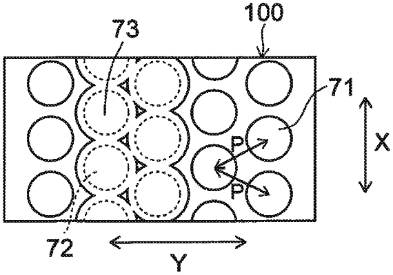
a plurality of columnar portions penetrating through the stacked body in the stacking direction, and each including a semiconductor film extending in the stacking direction and a cylindrical film provided between the electrode layers and the semiconductor film, the plurality of columnar portions including first columnar portions penetrating through the first portion of the stacked body in the stacking direction and second columnar portions penetrating through the second portion of the stacked body in the stacking direction,
the pair of sidewalls including a sidewall on the first portion side and a sidewall on the second portion side,
first concave portions being disposed at the sidewall on the first portion side along the first direction and second concave portions being disposed at the sidewall on the second portion side along the first direction,
in a transversal cross section of the first and second portions of the stacked body orthogonal to the stacking direction, the first columnar portions being provided in first openings of the first portion of the stacked body respectively and the second columnar portions being provided in second openings of the second portion of the stacked body respectively,
the first openings and third openings corresponding to the first concave portions being periodically arrayed in the transversal cross section, each of the first concave portions in the transversal cross section being a part of a corresponding third opening of the third openings respectively, and the second openings and fourth openings corresponding to the second concave portions being periodically arrayed in the transversal cross section, each of the second concave portions in the transversal cross section being a part of a corresponding fourth opening of the fourth openings respectively, and
a width in the second direction between the pair of sidewalls being larger than a diameter of the first openings and a diameter of the second openings.
|