| CPC H10B 43/27 (2023.02) [H01L 23/5283 (2013.01); H10B 41/27 (2023.02); H10B 41/35 (2023.02); H10B 43/35 (2023.02)] | 8 Claims |
|
1. A semiconductor memory device comprising:
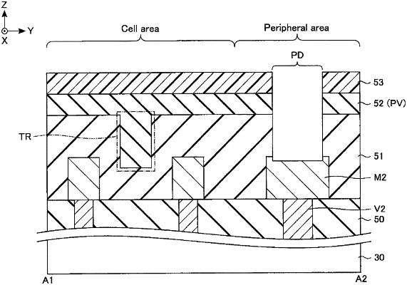
a memory cell array that includes a plurality of first interconnect layers and a first memory pillar, the first interconnect layers extending in a first direction substantially parallel to a semiconductor substrate, and the first memory pillar passing through the first interconnect layers and extending in a second direction substantially perpendicular to the semiconductor substrate;
a passivation film above the memory cell array;
a plurality of first insulating pattern layers above the passivation film, the first insulating pattern layers extending in the first direction and at least above the memory cell array, and arranged side by side in a third direction that is substantially parallel to the semiconductor substrate and intersects the first direction; and
a plurality of second insulating pattern layers above the passivation film, the second insulating pattern layers extending in the third direction and at least above the memory cell array, and arranged side by side in the first direction.
|