| CPC H10B 43/27 (2023.02) [G11C 16/08 (2013.01); H10B 43/10 (2023.02); H10B 43/35 (2023.02)] | 15 Claims |
|
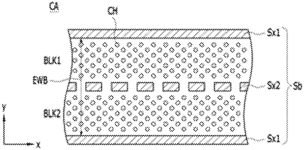
10. A semiconductor memory device comprising:
a slit structure configured to divide a plurality of memory blocks,
wherein the slit structure comprises first and second slit portions alternately arranged and extending parallel to each other in a first direction, and third and fourth slit portions extending parallel to each other in a second direction perpendicular to the first direction, the third slit portion configured to connect first ends of the first and second slit portions with each other, and the fourth slit portion configured to connect second ends of the first and second slit portions with each other,
wherein the first slit portion comprises a slit region, and
wherein the second slit portion has a dashed shape including the slit region and at least one bridge region.
|