| CPC H10B 41/35 (2023.02) [G11C 16/08 (2013.01); H01L 25/0657 (2013.01); H10B 41/20 (2023.02)] | 20 Claims |
|
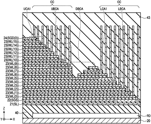
20. A semiconductor memory device, comprising:
a first memory cell region that includes a plurality of first conductor layers stacked in a first direction, a first semiconductor layer extending in the first direction through the plurality of first conductor layers;
a second memory cell region that is disposed in a second direction intersecting the first direction of the first memory cell region, and includes a plurality of second conductor layers stacked along the first direction, a second semiconductor layer extending in the first direction through the plurality of second conductor layers;
a connection region that is disposed between the first memory cell region and the second memory cell region and includes a plurality of third conductor layers stacked in the first direction and a first contact plug electrically insulated from the plurality of third conductor layers and extending in the first direction, each of the plurality of third conductor layers electrically connecting one layer of the plurality of first conductor layers and one layer of the plurality of second conductor layers; and
a row decoder that is disposed below the connection region and is configured to propagate a voltage to word lines of the first and second memory cell regions via the connection region electrically connected to the first contact plug of the connection region.
|