US 11,744,064 B2
Semiconductor circuit and electronic apparatus
Yasuo Kanda, Kanagawa (JP)
Assigned to SONY SEMICONDUCTOR SOLUTIONS CORPORATION, Kanagawa (JP)
Appl. No. 17/431,201
Filed by Sony Semiconductor Solutions Corporation, Kanagawa (JP)
PCT Filed Feb. 18, 2020, PCT No. PCT/JP2020/006281
§ 371(c)(1), (2) Date Aug. 16, 2021,
PCT Pub. No. WO2020/189147, PCT Pub. Date Sep. 24, 2020.
Claims priority of application No. 2019-048576 (JP), filed on Mar. 15, 2019.
Prior Publication US 2022/0149055 A1, May 12, 2022
Int. Cl. G11C 17/16 (2006.01); H10B 20/20 (2023.01); G11C 17/18 (2006.01)
CPC H10B 20/20 (2023.02) [G11C 17/16 (2013.01); G11C 17/18 (2013.01)] 15 Claims
OG exemplary drawing
 
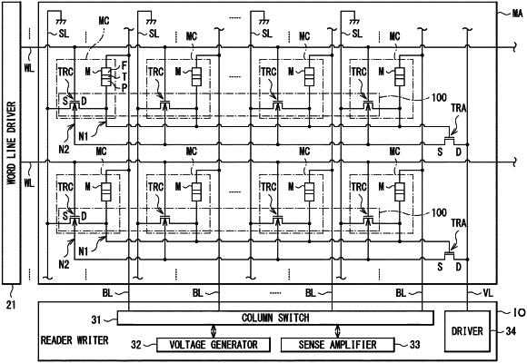
1. A semiconductor circuit comprising:
a first memory element including a first terminal, a second terminal coupled to a first node, and a tunnel barrier film, and configured to store information by breaking the tunnel barrier film;
a first transistor including a drain coupled to the first node, a source, a gate, and a back gate coupled to a second node; and
a second transistor including a drain, a source coupled to the second node, and a gate coupled to the first node.