| CPC H05K 7/20445 (2013.01) [H01L 23/3675 (2013.01); H01L 25/18 (2013.01); H05K 1/181 (2013.01); H05K 7/20509 (2013.01); H01R 12/716 (2013.01); H05K 2201/10015 (2013.01); H05K 2201/10159 (2013.01); H05K 2201/10189 (2013.01)] | 16 Claims |
|
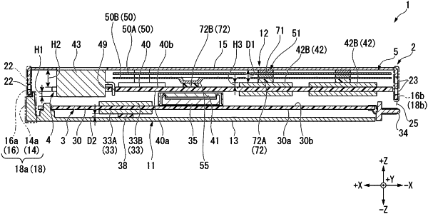
1. A semiconductor storage device, comprising:
a housing including a first wall;
a first substrate facing the first wall in the housing, one or more first electronic components being mounted on the first substrate, one or more second electronic components being arranged on the first substrate and having a greater height than the first electronic components with respect to the first substrate;
a plurality of heat radiating plates arranged between the first substrate and the first wall in the housing above the first substrate in a thickness direction of the first substrate; and
one or more connectors that connect the first substrate and the plurality of heat radiating plates, wherein one of the connectors is in direct contact with one of the first electronic components,
wherein the heat radiating plates are disposed at heights lower than the height of the second electronic components.
|