| CPC H05K 3/0026 (2013.01) [H05K 3/0014 (2013.01); H05K 3/185 (2013.01); H05K 3/188 (2013.01); H05K 3/28 (2013.01); H05K 3/423 (2013.01); H05K 3/4644 (2013.01); H05K 3/4652 (2013.01); H05K 2201/09018 (2013.01); H05K 2201/09118 (2013.01); H05K 2201/09827 (2013.01); H05K 2201/09854 (2013.01); H05K 2203/0582 (2013.01); H05K 2203/0588 (2013.01); H05K 2203/072 (2013.01); H05K 2203/107 (2013.01); Y10T 29/49124 (2015.01); Y10T 29/49155 (2015.01); Y10T 29/49165 (2015.01)] | 7 Claims |
|
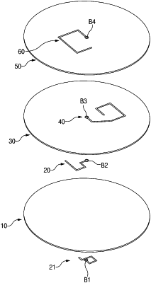
1. A method of forming a multi-layer circuit on a curved substrate, the method comprising:
forming, by a laser direct structuring process, a first layer of the multi-layer circuit on a first surface of the curved substrate;
applying a first layer of paint to the first layer of the multi-layer circuit;
forming; by the laser direct structuring process, a second layer of the multi-layer circuit on the first layer of the paint, the second layer of the multi-layer circuit being electrically coupled to the first layer of the multi-layer circuit;
applying a second layer of the paint over the second layer of the multi-layer circuit; and
forming, by the laser direct structuring process, a third layer of the multi-laver circuit on the second layer of the paint, the third layer of the multi-layer circuit being electrically coupled to the second layer of the multi-layer circuit.
|