| CPC H05K 1/09 (2013.01) [H05K 1/028 (2013.01); H05K 1/0393 (2013.01); H05K 1/181 (2013.01); H05K 3/28 (2013.01); H05K 3/3452 (2013.01); H05K 1/111 (2013.01); H05K 1/18 (2013.01); H05K 1/189 (2013.01); H05K 3/244 (2013.01); H05K 2201/0154 (2013.01); H05K 2201/0191 (2013.01); H05K 2201/0338 (2013.01); H05K 2201/10136 (2013.01)] | 17 Claims |
|
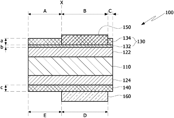
1. A flexible printed circuit board (FPCB), comprising:
a base;
a first metal layer and a second metal layer on respective surfaces of the base;
a first plating layer on the first metal layer;
a second plating layer under the second metal layer;
a first insulating pattern provided on the first plating layer; and
a second insulating pattern under a part of the second plating layer,
wherein a thickness of the first plating layer between the first insulating pattern and the base is less than a thickness of the second plating layer between the second insulating pattern and the base, and
wherein an upper surface of the first plating layer has a step portion, and a lower surface of the second plating layer does not have a step portion.
|