| CPC H05K 1/0298 (2013.01) [H05K 1/036 (2013.01); H05K 1/115 (2013.01); H05K 1/185 (2013.01); H05K 1/0366 (2013.01); H05K 1/111 (2013.01); H05K 2201/0141 (2013.01)] | 19 Claims |
|
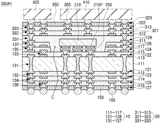
1. A printed circuit board, comprising:
a first insulating layer having a first modulus;
a second insulating layer disposed on the first insulating layer and having a second modulus;
a cavity penetrating the second insulating layer without penetrating the first insulating layer; and
a first wiring layer disposed on or in the first insulating layer,
wherein at least a portion of the first wiring layer protrudes from the first insulating layer into the cavity toward the second insulating layer,
wherein the second modulus is greater than the first modulus, and
wherein an edge portion of a bottom surface of the cavity is formed of an insulating material.
|