| CPC H05B 45/30 (2020.01) [G11C 16/0483 (2013.01); G11C 16/06 (2013.01)] | 18 Claims |
|
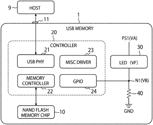
1. An electronic device comprising:
a light-emitting element having one end connected to a first voltage source;
a controller, connected between an other end of the light-emitting element and a host computer, and configured to control an emission of light from the light-emitting element based on a signal from the host computer; and
a resistance element connected between a first connecting portion and a reference potential source, the first connecting portion located between the light-emitting element and the controller, wherein the resistance element is provided to bypass at least part of a leakage current from the light emitting element and allow the leakage current to escape to the ground when the light emitting element is in an OFF state.
|