| CPC H04N 25/59 (2023.01) [H01L 27/14612 (2013.01); H04N 25/766 (2023.01); H01L 27/14643 (2013.01)] | 16 Claims |
|
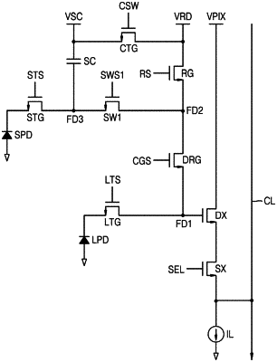
1. A unit pixel circuit, comprising:
a first photodiode;
a second photodiode different from the first photodiode;
a first floating diffusion node configured to accumulate charges generated in the first photodiode;
a second floating diffusion node configured to accumulate charges generated in the second photodiode;
a capacitor connected to the first floating diffusion node and a first voltage node, the capacitor configured to accumulate overflowed charges of the first photodiode;
a first switch transistor connecting the first floating diffusion node to a third floating diffusion node;
a reset transistor connecting the third floating diffusion node to a second voltage node;
a gain control transistor connecting the second floating diffusion node to the third floating diffusion node; and
a second switch transistor connected to both the first voltage node and the second voltage node.
|