| CPC H04N 25/00 (2023.01) [G06F 21/72 (2013.01); G09C 1/00 (2013.01); H01L 27/14634 (2013.01); H01L 27/14636 (2013.01); H04N 25/633 (2023.01); H04L 9/3231 (2013.01); H04N 25/65 (2023.01); H04N 25/67 (2023.01)] | 20 Claims |
|
1. A solid-state imaging device adapted to encrypt data, the solid-state imaging device comprising:
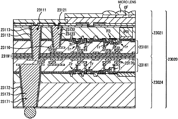
a sensor die comprising an array of imaging pixels formed on a first side of the sensor die and first wiring layers formed on a second side of the sensor die, wherein at least one of the imaging pixels is configured to generate specific signals, the specific signals being based on a physically unclonable function, the specific signals not output as an imaging result of the solid-state imaging device, wherein generating the specific signals not output as the imaging result of the solid-state imaging device comprises:
reading stored position information for each pixel block of a plurality of pixel blocks configured to generate pixel values that are not included within a range surrounding an average pixel value; and
using the stored position information for each pixel block, acquiring a respective pixel value for the pixel block;
a logic die comprising second wiring layers formed on a first side of the logic die; and
an encryption processor on the logic die configured to generate encrypted data using the specific signals, wherein the first side of the logic die is mounted adjacent to the second side of the sensor die and the first wiring layers electrically connect to the second wiring layers, wherein the at least one of the imaging pixels, the encryption processor, and a connecting conductor in which the specific signals pass through from the at least one of the imaging pixels to the encryption processor are located interior to the solid-state imaging device.
|