| CPC H03K 17/6872 (2013.01) [G06F 1/10 (2013.01); G06F 1/305 (2013.01); H03K 19/017509 (2013.01); H03L 7/0812 (2013.01)] | 8 Claims |
|
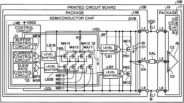
1. A data transmission device comprising:
a clock driver configured to issue a clock signal;
a buffer circuit configured to set a voltage level of a data signal to high or low, the data signal being issued according to the clock signal;
a buffer control circuit configured to control a switching operation of the buffer circuit;
a current circuit configured to make a dummy current flow from a first end of the current circuit to a second end thereof, the second end being connected to a ground line;
a power supply line connected to the first end of the current circuit and by which a power supply voltage is applied to the buffer circuit and the current circuit; and
a current control circuit configured to control the current circuit to make the dummy current flow during a time period no current is flowing in the buffer circuit, based on one of the set voltage level and a transmission timing of the data signal, wherein
the current circuit is configured to make the dummy current flow before the data signal is issued according to the clock signal.
|