| CPC H02J 7/00047 (2020.01) [H02J 7/0031 (2013.01); H02J 7/00036 (2020.01); H01M 10/4257 (2013.01); H02J 7/00302 (2020.01)] | 8 Claims |
|
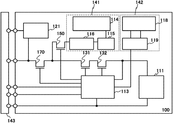
1. A power storage device comprising:
a power receiving circuit;
a power storage unit;
a first transistor between the power receiving circuit and the power storage unit;
a second transistor between the first transistor and the power storage unit;
a third transistor between the second transistor and the power storage unit; and
a control circuit electrically connected to a gate of the first transistor, a gate of the second transistor, a gate of the third transistor, and the power storage unit,
wherein the power receiving circuit is electrically connected to a one of a source and a drain of the first transistor,
wherein the other one of the source and the drain of the first transistor is electrically connected to a one of a source and a drain of the second transistor,
wherein the other one of the source and the drain of the second transistor is electrically connected to a one of a source and a drain of the third transistor,
wherein the other one of the source and the drain of the third transistor is electrically connected to the power storage unit,
wherein the second transistor is configured to serve as a protection switch for preventing overcharge of the power storage unit,
wherein the third transistor is configured to serve as a protection switch for preventing over-discharge of the power storage unit, and
wherein the control circuit includes:
a first memory circuit configured to hold data in a period during which power is supplied to the control circuit from the power storage unit; and
a second memory circuit configured to hold data in a period during which supply of the power to the control circuit from the power storage unit is stopped.
|