| CPC H01S 5/1042 (2013.01) [H01S 3/0933 (2013.01); H01S 5/041 (2013.01); H01S 5/1067 (2013.01); H01S 5/11 (2021.01); H01S 5/30 (2013.01); H01L 33/58 (2013.01); H01L 2933/0058 (2013.01); H01L 2933/0083 (2013.01); H01S 5/026 (2013.01)] | 20 Claims |
|
13. A laser structure including a monolithically formed nanocavity laser and light emitting diode (LED), comprising:
a substrate including silicon (Si) or germanium (Ge);
a buffer layer including a III-V material and having a first surface formed on the substrate;
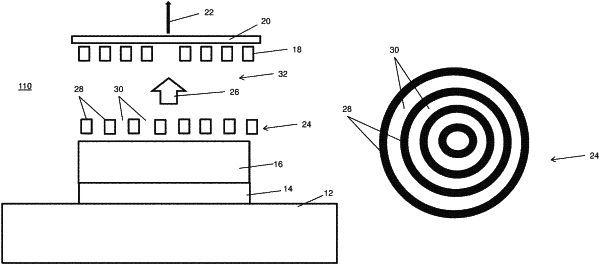
a light emitting diode (LED) formed on a second surface of the buffer layer and configured to produce visible light;
a lens disposed on the LED to focus the visible light to output focused light;
a photonic crystal layer formed on the LED to receive the focused light; and
a nanocavity laser formed on the photonic crystal layer, is a monolayer of a transition metal dichalcogenide having a chemical formula of MX2 for receiving the focused light through the photonic crystal layer to optically pump the nanocavity laser, where M is selected from the group consisting of: W and Mo and X is selected from the group consisting of: S, Se and Te; wherein the buffer layer further includes an interface material to reduce dislocation defects due to lattice mismatch between the substrate and the buffer layer.
|