US 11,742,631 B1
Facet on a gallium and nitrogen containing laser diode
James W. Raring, Santa Barbara, CA (US); Hua Huang, Vancouver, WA (US); Phillip Skahan, Santa Barbara, CA (US); Sang-Ho Oh, Goleta, CA (US); Ben Yonkee, Fremont, CA (US); Alexander Sztein, Santa Barbara, CA (US); and Qiyuan Wei, Fremont, CA (US)
Assigned to KYOCERA SLD Laser, Inc., Goleta, CA (US)
Filed by KYOCERA SLD Laser, Inc., Goleta, CA (US)
Filed on Sep. 16, 2021, as Appl. No. 17/476,776.
Application 17/476,776 is a continuation of application No. 16/786,551, filed on Feb. 10, 2020, granted, now 11,139,634, issued on Oct. 5, 2021.
Application 16/786,551 is a continuation of application No. 15/937,740, filed on Mar. 27, 2018, granted, now 10,559,939, issued on Feb. 11, 2020.
Application 15/937,740 is a continuation in part of application No. 15/789,413, filed on Oct. 20, 2017, granted, now 11,121,522, issued on Sep. 14, 2021.
Application 15/789,413 is a continuation of application No. 15/153,554, filed on May 12, 2016, granted, now 9,800,016, issued on Oct. 24, 2017.
Application 15/153,554 is a continuation in part of application No. 13/850,187, filed on Mar. 25, 2013, granted, now 9,343,871, issued on May 17, 2016.
Claims priority of provisional application 61/620,648, filed on Apr. 5, 2012.
This patent is subject to a terminal disclaimer.
Int. Cl. H01S 5/028 (2006.01); H01S 5/02 (2006.01); H01S 5/042 (2006.01); H01S 5/343 (2006.01); H01S 5/32 (2006.01); H01S 5/20 (2006.01); H01S 5/22 (2006.01)
CPC H01S 5/0287 (2013.01) [H01S 5/0203 (2013.01); H01S 5/0282 (2013.01); H01S 5/0425 (2013.01); H01S 5/34333 (2013.01); H01S 5/2009 (2013.01); H01S 5/22 (2013.01); H01S 5/3202 (2013.01); H01S 2304/04 (2013.01)] 20 Claims
OG exemplary drawing
 
1. A laser device, comprising:
a substrate having a surface;
a gallium and nitrogen containing cavity region overlying the surface, the gallium and nitrogen containing cavity region characterized by a first end and a second end, the first end comprising a first etched facet and the second end comprising a second etched facet; and
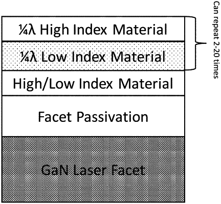
a passivation layer comprising a polycrystalline layer of Al2O3 directly contacting the first etched facet, wherein an interface between the passivation layer and the first etched facet is substantially contaminant free.