| CPC H01Q 1/2283 (2013.01) [H01L 21/4853 (2013.01); H01L 21/4857 (2013.01); H01L 21/565 (2013.01); H01L 21/568 (2013.01); H01L 21/6835 (2013.01); H01L 23/3128 (2013.01); H01L 23/49816 (2013.01); H01L 23/49822 (2013.01); H01L 23/49838 (2013.01); H01L 23/552 (2013.01); H01L 23/66 (2013.01); H01L 24/08 (2013.01); H01L 24/16 (2013.01); H01L 24/81 (2013.01); H01L 25/16 (2013.01); H01Q 1/50 (2013.01); H01Q 21/24 (2013.01); H01L 2221/68359 (2013.01); H01L 2223/6677 (2013.01); H01L 2224/08237 (2013.01); H01L 2224/16227 (2013.01); H01L 2224/80006 (2013.01); H01L 2924/19102 (2013.01); H01L 2924/3025 (2013.01)] | 20 Claims |
|
1. A semiconductor device, comprising:
a substrate comprising:
a substrate top side;
a substrate bottom side;
a substrate dielectric structure between the substrate top side and the substrate bottom side; and
a substrate conductive structure traversing the substrate dielectric structure and comprising:
a first substrate terminal; and
a second substrate terminal at the substrate top side;
an electronic component coupled to the substrate and comprising:
a component terminal coupled to the first substrate terminal; and
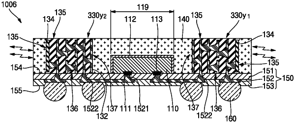
a first antenna element coupled to the substrate and comprising:
a first element head side;
a first element dielectric structure;
a first element conductive structure comprising a first element terminal and contacting the first element dielectric structure; and
a first antenna pattern at the first element head side and grouped with the first element terminal and the first element conductive structure;
wherein:
the first antenna element is coupled to the substrate outside a footprint of the electronic component; and
the first element terminal is coupled to the second substrate terminal; and
wherein:
the first element head side comprises a lateral side of the first antenna element; and
the first antenna pattern is on the lateral side of the first antenna element and is configured to radiate in a lateral direction perpendicular to the lateral side of the first antenna element.
|